

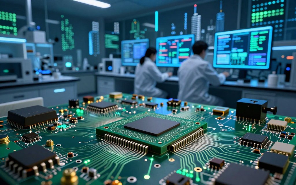
Silicon technology uses engineering and manufacturing methods to create essential electronic components and silicon-based devices. What is silicon technology? It uses silicon-based semiconductors in processors, memory units, sensors, and solar cells. Its special properties make it central to the modern digital world.
Silicon is a highly effective semiconductor with several useful advantages. It is abundant, cost-effective, and works well with precise manufacturing methods. This semiconductor technology supports telecommunications, consumer electronics, and connected devices used in daily life.
Silicon technology explained: This article covers silicon’s atomic structure and the details of wafer manufacturing. It also examines silicon’s key roles in computing and telecommunications, plus its importance to the U.S. industrial sector. Finally, it looks toward advanced process nodes and silicon photonics.
Key Takeaways
- Silicon serves as the foundation for various electronic components.
- Its semiconductor properties make it crucial for modern devices.
- Silicon is abundant and cost-effective, supporting large-scale production.
- The technology plays a significant role in telecommunications and computing.
- Future advancements include developments in silicon photonics and process nodes.
The Origins and Discovery of Silicon as a Technological Material
Silicon moved from a scientific curiosity to an important silicon material for technology. Its story began in the early 19th century, as scientists studied this element’s unusual properties. At first, researchers knew silicon mainly through compounds, while pure silicon remained hard to isolate.
Early Scientific Discovery of Silicon in the 19th Century
The history of silicon reaches back to 1824, when Swedish chemist Jöns Jacob Berzelius isolated relatively pure silicon. His work marked a major step in 19th-century chemistry and supported later studies of silicon’s properties. Before then, scientists mainly found silicon in silicates, compounds made from silicon and oxygen.
“Silicon is the backbone of modern electronics, a testament to the transformative power of scientific discovery.”
After isolation, silicon entered glass and ceramics. These industrial silicon applications helped reveal its value beyond basic materials.
Transition from Industrial Applications to Electronic Uses
As the 20th century approached, better crystal growth and electrical theory revealed silicon’s value as a semiconductor. The invention of the transistor in the 1940s showed this shift and relied heavily on silicon’s semiconductor properties.
Later, integrated circuits placed silicon at the center of modern computing and communications. This change did more than create new uses; it transformed industries and daily life.
Related Posts:




| Year | Discovery/Application | Scientist/Company |
|---|---|---|
| 1824 | Isolation of Silicon | Jöns Jacob Berzelius |
| 1947 | Invention of the Transistor | Bell Labs |
| 1958 | First Integrated Circuit | Jack Kilby |
These advances changed silicon from an industrial material into an electronic-age cornerstone, proving its versatility and essential role in technology.
What Is Silicon Technology and Why It Matters Today
What is silicon technology? It is more than a material; it is a system supporting our digital age. It includes materials, processes, devices, and systems built around silicon semiconductor technology. These range from purified silicon wafers to transistor fabrication, integrated circuits, and electronic-device packaging.
Modern engineering uses silicon technology in telecommunications, computing, and automotive electronics. Silicon can conduct electricity efficiently and also act as an insulator, making it vital to electronic engineering. The U.S. semiconductor industry depends on it to compete in global markets.
Silicon technology matters for more than the economy. It supports national security and affects artificial intelligence, cloud computing, and defense systems. A strong semiconductor supply chain helps the United States protect technological independence and resist global disruptions.
The United States must invest in domestic research, chip design, and fabrication capacity. Skilled workers and advanced manufacturing techniques can strengthen its semiconductor supply chain. This proactive approach supports the economy and protects the nation’s technological future.
The Atomic Structure and Semiconductor Properties of Silicon
Silicon atomic structure makes it a key material in semiconductor technology. As element 14 on the periodic table, silicon belongs to Group 14 and has four valence electrons. The stable crystalline lattice also allows precise changes, making silicon ideal for electronic applications.
Silicon’s Position on the Periodic Table and Atomic Bonding
Silicon’s position on the periodic table shapes its bonding behavior. Each atom forms covalent bonds with four other silicon atoms, creating a three-dimensional network. The strength of these bonds helps preserve silicon’s integrity as a semiconductor and lets it conduct electricity under certain conditions.
Electrical Conductivity, Band Gap, and Doping Behavior
Silicon has an indirect silicon band gap of about 1.12 electron volts at room temperature. This band gap affects electrical conductivity and optical behavior, while doping adds donor or acceptor atoms. Pure silicon conducts weakly; semiconductor doping creates n-type and p-type materials and can improve conductivity.
These dopants create p-n junctions, the building blocks of semiconductor devices such as diodes, transistors, and solar cells. Manufacturers control doping to tailor silicon’s electrical properties for integrated circuits and other electronic components.
In summary, silicon atomic structure and semiconductor properties support its central role in modern technology. These features show silicon’s importance and drive ongoing innovation in semiconductor applications.
For more detailed information about silicon, visit this link.
How Silicon Is Extracted and Purified for Electronics Manufacturing
Learning about silicon purification explains how electronics manufacturing works. Most silicon comes from silica found in quartz and other silicon dioxide forms. This process creates high-quality materials needed for modern electronics.
From Silica Sand to Metallurgical-Grade Silicon
Silica sand, made mostly of silicon dioxide, begins silicon production. In an electric arc furnace, carbon reduces silica into metallurgical-grade silicon. This silicon serves some industrial uses but lacks purity for advanced electronics.
Achieving Semiconductor-Grade Purity Through Refinement
Reaching semiconductor-grade silicon requires further refinement. These steps support polysilicon production:
- Conversion of metallurgical-grade silicon into volatile silicon compounds.
- Distillation processes to separate impurities.
- Chemical vapor deposition to create polysilicon.
Even trace metallic or atomic impurities can affect transistor performance, leakage current, yield, and reliability. Silicon purification is only the first requirement. During wafer production, manufacturers also control crystal defects, oxygen levels, carbon concentration, surface flatness, and contamination.
| Purity Level | Impurity Concentration | Application |
|---|---|---|
| Metallurgical-Grade Silicon | 1,000 ppm | Industrial Uses |
| Semiconductor-Grade Silicon | 1 ppm | Electronics Manufacturing |
| Solar-Grade Silicon | 10 ppm | Photovoltaic Cells |
The Wafer Fabrication Process: From Sand to Functional Chips
Silicon’s journey from raw material to working chips is complex and fascinating. This section explains silicon wafer fabrication, showing how purified silicon becomes the microelectronics powering modern devices.
Crystal Growth and Ingot Formation
The first step in silicon wafer fabrication is crystal growth. The Czochralski process dips a small seed crystal into molten silicon, then slowly pulls it upward. This forms a cylindrical ingot of single-crystal silicon; the efficient method produces high-quality crystals and is widely used.
Float-zone processing is another method for crystal growth. It offers higher purity, making it ideal for specialized applications. Workers melt a silicon rod in a controlled environment, separating impurities from the growing crystal.
Both methods produce ingots later sliced into thin wafers.
Czochralski Process and Float-Zone Techniques
| Technique | Purity Level | Typical Applications |
|---|---|---|
| Czochralski Process | High | General semiconductor applications |
| Float-Zone Technique | Very High | Specialized electronic devices |
Photolithography, Etching, and Transistor Patterning
After preparing the silicon wafers, front-end manufacturing begins. Photolithography transfers circuit patterns onto wafers using photosensitive resist and light exposure. The pattern shows where workers will deposit materials or etch them away.
After photolithography, etching removes unprotected silicon areas and creates intricate circuit designs. This step is crucial for transistor manufacturing because it shapes integrated circuits’ basic components.
Deposition, Ion Implantation, and Metallization
After etching, deposition builds insulating, conducting, and semiconducting layers on the wafer. Ion implantation adds controlled dopants, changing silicon’s electrical properties and forming p-type or n-type regions. These regions are essential for transistor function.
Finally, metallization creates electrical connections between transistors, helping them communicate. The process needs precise alignment and control because small errors can cause major defects in finished chips.
After fabrication, workers inspect wafers and perform rigorous electrical tests. They then dice, package, and test individual chips again to ensure functionality. Wafer fabrication blends science and engineering, creating technology that powers our digital world.
Key Components Built on Silicon Technology
Silicon technology supports many critical components in modern electronics. This versatile material has driven innovations beyond traditional computing devices. Today, we will explore key components built on silicon technology and their uses in different fields.
Integrated Circuits and Microprocessors
Integrated circuits (ICs) are fundamental to modern electronics. They combine transistors, capacitors, resistors, and interconnects on one substrate for compact, reliable systems. These circuits build microprocessors, programmable logic engines for computers, vehicles, and industrial equipment.
Microprocessors are essential for executing instructions and processing data. They perform complex calculations quickly, making technology smarter and more efficient. They power smartphones and embedded systems and play a vital role in daily life.
Sensors, Photovoltaic Cells, and MEMS Devices
Silicon sensors support many sensing applications. Image sensors, pressure sensors, accelerometers, and gyroscopes are integral to many devices. They enable motion detection and environmental monitoring, improving user experience and safety.
Photovoltaic cells use silicon’s semiconductor properties to convert sunlight into electricity. This technology supports renewable energy solutions and a sustainable future. Improved efficiency has made silicon photovoltaic cells more accessible and cost-effective.
Microelectromechanical systems (MEMS) devices are another innovative use of silicon technology. They combine microscopic mechanical structures with electronic circuits for advanced functions in compact forms. These devices serve motion detection, microphones, medical instruments, and automotive safety systems.
| Component Type | Application | Key Features |
|---|---|---|
| Integrated Circuits | Computers, smartphones | Compact, reliable |
| Microprocessors | Embedded systems, vehicles | Programmable, efficient |
| Silicon Sensors | Motion detection, monitoring | High sensitivity |
| Photovoltaic Cells | Solar energy systems | Renewable, efficient |
| MEMS Devices | Medical instruments, automotive | Compact, multifunctional |
Silicon Technology in Computing: CPUs, GPUs, and Memory
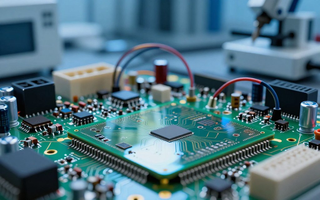
Silicon technology powers computing systems, from smartphones to supercomputers. It supports efficiency through computer chips and semiconductor processors. This section examines Central Processing Units (CPUs), Graphics Processing Units (GPUs), DRAM, and NAND flash storage.
Central Processing Units and Graphics Processing Units
CPUs act as the brain of any computing device, executing instructions and managing tasks. They handle basic operations and complex calculations.
GPUs are specialized processors built for parallel processing. Silicon GPUs excel at rendering graphics and support machine learning and scientific computations.
Both CPUs and GPUs use advanced silicon technology to improve performance. These improvements come from three main approaches:
- Transistor Scaling: As transistors become smaller, more can fit onto a chip, enhancing performance and energy efficiency.
- Parallel Processing: GPUs utilize many cores to process multiple tasks simultaneously, making them ideal for data-intensive applications.
- Architecture Optimization: The design of silicon chips is continually refined to improve speed and efficiency.
Memory Chips Including DRAM and NAND Flash Storage
Memory strongly affects computing performance. DRAM (Dynamic Random Access Memory) is volatile memory that briefly stores active data and instructions. This lets CPUs access information quickly and keeps systems running smoothly.
NAND flash storage is non-volatile memory used in solid-state drives (SSDs), smartphones, and other devices. It retains data even when powered off, making it essential for long-term storage. Using DRAM memory and NAND flash storage together improves:
- Speed: Faster access to data improves overall system performance.
- Efficiency: Modern architectures optimize memory bandwidth to support demanding applications.
- Capacity: Larger memory sizes enable more applications to run simultaneously without slowdowns.
Together, silicon CPUs, GPUs, and memory chips shape modern computing performance. As technology advances, these components will become more efficient and powerful, shaping computing’s future.
Silicon Technology in Telecommunications and Networking
Silicon technology plays a key role in modern telecommunications and networking. Its uses support information transmission, processing, and conversion across many platforms. This section explains how silicon RF chips and silicon photonics improve communication systems.
RF Chips and Signal Processing Components
RF chips are vital in telecommunications. They generate, receive, filter, amplify, and convert wireless signals. These chips appear in smartphones, Wi-Fi equipment, satellite systems, and cellular infrastructure while supporting smooth communication through efficient signal processing.
Mixed-signal circuits connect analog signals with digital processing. This design improves signal clarity, reduces interference, and makes communication more reliable. Industry experts say, “The advancement of RF chip technology is pivotal for the future of wireless communication.”
Fiber Optic Networks and Silicon Photonics
Fiber optic networks are changing data transmission through high-speed communication. Silicon photonics uses silicon-based optical components to guide, modulate, detect, and switch light for efficient data transfer. This technology supports data centers, cloud services, and high-bandwidth communications.
Silicon photonics works with materials such as compound semiconductors for specialized optical functions. For example, silicon guides light well, but lasers may need other materials for best performance. This hybrid approach improves the efficiency of telecommunications semiconductors.
Integrating silicon technology into telecommunications and networking improves communication systems and supports future innovations. Demand for faster, more reliable communication continues to grow, so silicon remains essential in this sector.
Silicon Technology in Consumer Electronics and IoT Devices
Silicon technology shapes consumer electronics and the Internet of Things (IoT). It brings components together, helping devices become smarter and more efficient. From silicon in smartphones to smart home systems, chips drive performance and function.
Smartphones and tablets use several silicon components that work together. These include application processors, graphics engines, memory, storage controllers, image sensors, power-management integrated circuits (ICs), wireless chips, and security hardware. Together, these parts provide fast processing, stunning graphics, and reliable connectivity for a smooth user experience.
Smartphones, Tablets, and Wearable Devices
Wearable technology has benefited greatly from silicon advances. Smartwatches and fitness trackers use low-power processors, motion sensors, biometric sensors, and display drivers. These parts monitor health metrics, track physical activity, and send real-time notifications while preserving long battery life.
The compact design of these devices comes from miniaturized silicon components. This lets manufacturers create sleek, lightweight products that remain comfortable without losing useful functions.
Smart Home Systems and Connected Sensors
Smart home systems are another major use of silicon technology. These systems include smart home sensors, thermostats, cameras, locks, lighting controllers, and environmental sensors. Silicon chips support sensing, computation, communication, and security, helping homes stay efficient and secure.
Power efficiency is vital in IoT design. Silicon technology helps devices use less energy while handling complex tasks. Effective heat management prevents overheating, supporting smooth operation, longevity, and reliability.
Data privacy and reliable wireless connectivity also matter. Silicon chips support strong encryption and secure communication protocols, protecting user data in a connected world. This focus on security builds consumer trust in smart devices and connected electronics.
| Device Type | Silicon Components | Key Features |
|---|---|---|
| Smartphones | Application Processors, Graphics Engines | High-speed processing, Stunning graphics |
| Wearable Devices | Low-power Processors, Biometric Sensors | Health monitoring, Activity tracking |
| Smart Home Systems | Environmental Sensors, Security Chips | Energy efficiency, Enhanced security |
Silicon technology is fundamental to consumer electronics and IoT devices. It combines functions in compact packages, improving user experience and encouraging innovation. As technology evolves, silicon will remain central to the future of connected devices.
Why Silicon Remains Dominant Over Alternative Materials
Silicon remains the semiconductor industry’s leading material, despite growing interest in alternatives. Its established role in electronics comes from several proven advantages for manufacturers and designers.
Cost Efficiency and Manufacturing Scalability
One major reason is its cost efficiency. Silicon uses abundant, affordable raw materials, helping control the silicon manufacturing cost. This leads to lower overall silicon manufacturing costs and supports mass production.
Silicon technology also supports manufacturing scalability and semiconductor scalability. Large wafers produce many chips in one batch, which greatly reduces production costs. This capacity helps industries meet high semiconductor demand.
Established Fabrication Infrastructure in the U.S.
The U.S. fabrication infrastructure helps silicon keep its leading position. The country has a strong ecosystem of research institutions, skilled workers, and advanced factories. Together, they support innovation and keep silicon at the forefront of technology.
Performance Trade-offs with Germanium, Gallium Nitride, and Graphene
Silicon faces competition from germanium semiconductors, gallium nitride, and graphene electronics. Each alternative offers a distinct advantage:
| Material | Advantages | Challenges |
|---|---|---|
| Germanium | High carrier mobility | Integration and stability issues |
| Gallium Nitride | Excellent for high-power applications | Higher manufacturing costs |
| Graphene | Exceptional electrical properties | Lacks a useful band gap for digital applications |
These materials offer strong benefits, but they often complement silicon instead of replacing it. Silicon’s established infrastructure and proven performance keep it relevant in semiconductor technology.
The Future of Silicon Technology and Emerging Innovations
The future of silicon technology will bring major innovations that shape the next wave of computing. As chip makers move to smaller process nodes, such as 3nm chips and 2nm chips, they face major engineering challenges. These labels mark advanced process generations, showing modern chip design’s complexity, not a measurement of every transistor feature.
Each new generation makes leakage, heat dissipation, variability, interconnect resistance, and lithography harder to manage. Advanced process nodes need solutions such as gate-all-around transistor structures and backside power delivery. These technologies improve performance, control rising fabrication costs, and increase yield.
Moreover, silicon photonics innovation offers a key path to better data movement among processors, memory, and network equipment. By joining optical components with silicon, it can deliver faster data transfer and lower latency. These gains support the next generation of high-performance computing.
Another exciting frontier is quantum computing. Research on silicon-based quantum systems, such as silicon spin qubits, shows promise but brings major challenges. Researchers must solve problems with control, error correction, cooling, and manufacturing before quantum computing becomes mainstream.
“The future of silicon technology is not just about scaling down; it’s about integrating new paradigms to unlock unprecedented capabilities.”
In conclusion, silicon will remain a cornerstone of modern technology. Its future will likely combine traditional silicon applications with optical, compound-semiconductor, and quantum technologies. This evolution shows technology’s changing nature, as innovation drives progress and shapes the future.
Conclusion
Silicon technology supports modern digital electronics. Its unique semiconductor properties make it vital for applications ranging from integrated circuits to advanced processors. Turning raw silica into high-purity silicon wafers shows the remarkable growth of silicon semiconductor applications.
As we consider the silicon technology future, semiconductor innovation remains critical. Emerging fields such as quantum computing and silicon photonics show that silicon is not alone. Alternative materials like germanium and gallium nitride will serve essential roles in specialized applications.
Investment in U.S. semiconductor infrastructure will help maintain leadership in digital electronics. Better energy efficiency, advanced fabrication techniques, and innovative packaging solutions will shape the next generation of devices. A comprehensive silicon technology overview reveals a strong ecosystem supporting ongoing research and development.
In conclusion, silicon continues to dominate, but the materials landscape is changing. Staying ahead in this dynamic field requires commitment to innovation and adaptation. The future of digital systems depends on how well we harness silicon and its alternatives.